Enhanced RISC-based MIPS Processor
Overview
This project outlines the design of an enhanced RISC-based MIPS processor with increased memory capacity and I/O ports, based on the specifications provided in the documentation/DesignDocument.pdf research paper. The design aims to improve the performance and versatility of a standard MIPS architecture.
Key Enhancements
- Increased Memory: Target memory capacity of 4GB.
- Additional I/O Ports: Four I/O ports (PORTA, PORTB, PORTC, PORTD) for expanded device interaction.
- IEEE-754 FPU: Integration of a floating-point unit compliant with the IEEE-754 standard for robust handling of floating-point arithmetic.
Project Structure
Enhanced-RISC-MIPS/
├── README.md
├── documentation/
├── verilog/ (Placeholder)
├── testbenches/ (Placeholder)
├── images/
└── LICENSE
documentation/: Contains the DesignDocument.pdf detailing the architecture, design choices, and testing methodologies.verilog/: (Placeholder) Intended for the Verilog implementation of the processor modules. See the verilog/README.md for more information about planned module design.testbenches/: (Placeholder) Intended for Verilog testbenches used to verify the functionality of the processor modules. See the testbenches/README.md for the described testing approach.images/: Contains the figures included in the DesignDocument.pdf.
Key Figures
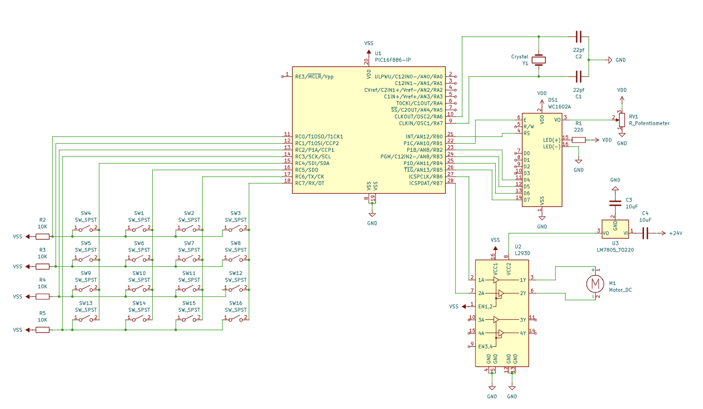
Circuit Diagram
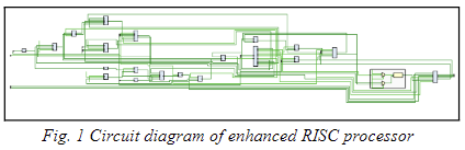
Figure 1: Circuit diagram of the enhanced RISC processor
CPU Memory Module
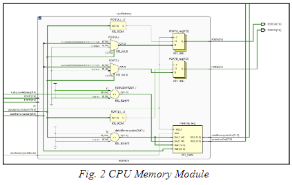
Figure 2: CPU Memory Module
Data Memory MUX Modules
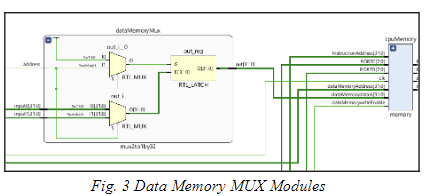
Figure 3: Data Memory MUX Modules
float MUX and float Reg Modules
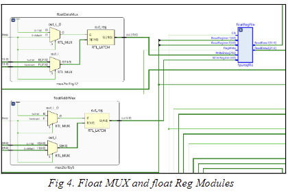
Figure 4: float MUX and float Reg Modules
ALU, fpu and opcode Decoder Modules
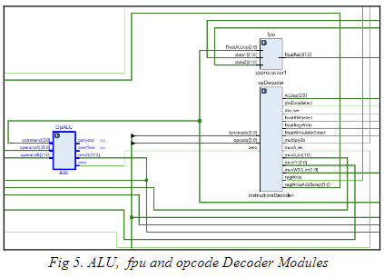
Figure 5: ALU, fpu and opcode Decoder Modules
MUX and Program Counter Modules
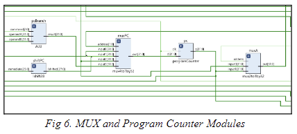
Figure 6: MUX and Program Counter Modules
Main Register, MUX, and Write Modules
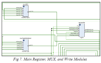
Figure 7: Main Register, MUX, and Write Modules
Sign Extension, MUX, and Multiply Modules
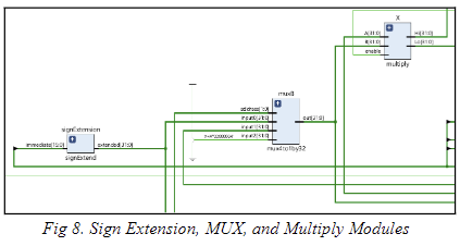
Figure 8: Sign Extension, MUX, and Multiply Modules
Addition and Subtraction of Floating Point Numbers
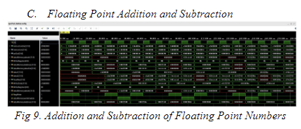
Figure 9: Addition and Subtraction of Floating Point Numbers
Multiplication and Division of Integers
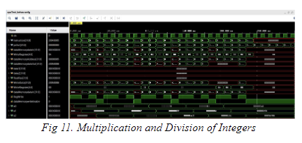
Figure 10: Multiplication and Division of Integers
I/O Ports Timing Simulation
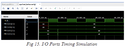
Figure 15: I/O Ports Timing Simulation
I/O Ports Schematic Diagram
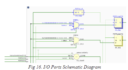
Figure 16: I/O Ports Schematic Diagram
Timing Diagram for Memory Addresses
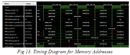
Figure 13: Timing Diagram for Memory Addresses
Data Memory Multiplexer
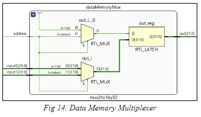
Figure 14: Data Memory Multiplexer
Planned Implementation (Verilog Directory)
(See verilog/README.md for a description)
Although Verilog code is not yet available, the following modules are envisioned for the complete implementation:
- CPU Core Modules: ALU, Control Unit, Register File, Memory Interface
- I/O Modules: Individual modules for PORTA, PORTB, PORTC, and PORTD, handling bidirectional data flow.
- FPU Modules: Modules for floating-point addition/subtraction, multiplication/division.
Planned Test Approach (Testbenches Directory)
(See testbenches/README.md for a description)
The testbenches are intended to ensure proper functioning of all the processor components
License
This project is licensed under the MIT License.